Modern electronics are reliant on microchips. At heart, a ‘microchip’ contains transistors; on their own, transistors are simple binary logic gates that can be ‘on’ or ‘off’, but can be combined and permuted into performing large, complex operations. The more transistors you can fit onto a microchip, the better. For example, The Apple M1 chip, manufactured by the Taiwan Semiconductor Manufacturing Company (TSMC) has an area of about 120mm2, and contains over 16 billion transistors. How is this even possible? In short, the answer is a massive laser, about the size of a room, shooting a droplet of metal and forming a tiny plasma, less than the width of a human hair.
The principle of printing something using a pattern is called lithography. This applies to art, but also to semiconductors. In semiconductor manufacturing, light is used to etch away substrate, leaving behind a pattern. the smaller your wavelength of light is, the smaller features you can produce. In the frame of lithography for semiconductors, this means fitting more transistors onto your chip.
The history of realising EUV lithography follows many aligning tracks, technologies and companies. Today, we’ll look at the underlying technologies.
The Laser
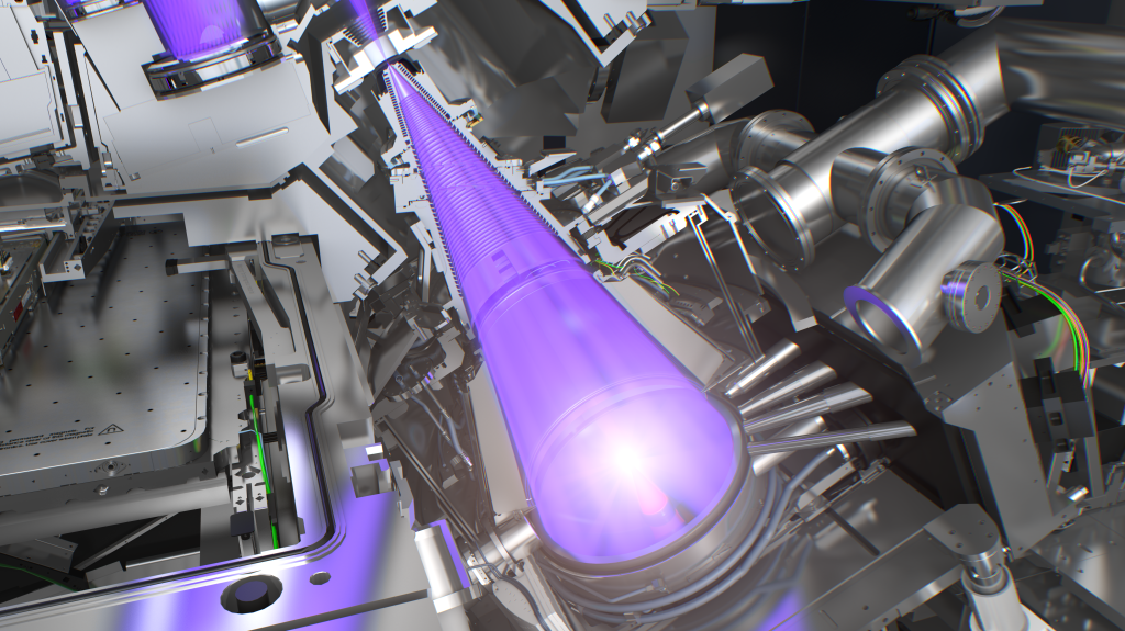
The driving laser in the EUV system is a 20-40kW CO2 laser, produced by TRUMPF. The laser alone weighs over 17 tonnes, and is so large it is placed below the collector and wafer system. Initially, two low Wattage seed laser pulses are amplified up to about 100W (we have to get this up to 40kW). They then pass through four more resonators, which amplify the pulse power further You can read more about the laser on TRUMPF’s website here.

The Optics
The optics used in the EUV lithography system reflect and move the light through the sytem In practice, each mirror only reflects about 70%, and so as the light propagates through the system, there are losses.
The Reticle
Let’s not forget that the system that’s being designed is a lithography system, so we need something that is to be printed.
The reticle, also referred to as the mask, is a patterned plate and is a magnified image of the transistor pattern that will ultimately comprise the circuitry. The EUV light passes through (or more accurately, reflects off) the reticle, projecting the design pattern onto the wafer below.
Because any imperfection in the mask would be replicated across millions of chips, it must be made with atomic-scale precision and kept extremely clean.
The Pellicle
As you can imagine, the tin droplets that are being irradiated with the source laser 50,000 times a second is a messy process; debris will naturally form. This can be in the form of tin atoms, ions or molecules, where tin ions bond with hydrogen in the system (which is used as a buffer gas, another story for another day). Debris can damage the system, including the wafer that you’re trying to coat
To protect the surface of the silicon wafer, a pellicle is placed between the reticle and the wafer. The pellicle is a thin, transparent membrane that acts like a shield, catching particles and preventing contamination from reaching the reticle pattern or wafer.
Developing pellicles for EUV is especially challenging because they must survive high temperatures and transmit extremely short-wavelength light with minimal absorption.
The Source
Each tin droplet is about 30 um in diameter and fired at a rate of tens of thousands per second. The CO₂ laser pulse first flattens the droplet into a thin disk, and then a second pulse strikes it again to form a laser-produced plasma with temperatures of around 200,000 °C.
This plasma emits light in the extreme ultraviolet (EUV) range—13.5 nm wavelength—ideal for creating features smaller than 10 nm on a chip.
Collecting this light efficiently is a major engineering challenge; special collector mirrors coated with multilayer materials gather the emitted EUV and direct it toward the projection optics and reticle.
The Mirrors
Unlike ordinary mirrors, which have a single reflective surface and reflect optical light, EUV mirrors are multilayer stacks—typically 40 to 50 alternating layers of molybdenum (Mo) and silicon (Si), each just a few nanometers thick and optimally designed to reflect 13.5 nm, plus or minus 1%.
They reflect EUV light reasonably efficiently—about 70% reflectivity. These mirrors, manufactured by Zeiss, are incredibly difficult to make. The surface roughness must be less than 0.1 nanometers, and the layers must be deposited with atomic precision. Any defect—dust, scratches, or even slight layer thickness variations—can scatter light or distort the image projected onto the wafer. Over 10 of these mirrors are placed inside an EUV source to direct the light onto the wafer.
The Future
The current EUV system is inefficient. Consider this; the CO2 laser produces 20-40kW. of light, but this requires 1 MW of power; that’s only a 2% wall plug efficiency! This laser then produces at most 250 W of EUV light. By the time the EUV light is reflected off each 70% EUV reflectivity mirror, through the mask and onto the pellicle, there’s, about 2W that are used to print the. This is at most a 0.01% efficiency – how can you make this better?
For one, moving to shorter wavelength system would be a great benefit. Shorter wavelength systems would be solid state, which typically have a higher wall plug efficiency. There are also physically beneficial reasons for moving to a wavelength that is shorter than the 10.6 um system offered by CO2 lasers, but that’s a story for a different day.
Learn more
There are many great resources to learn more about ASML’s laser plasma light source. For the global standard of industry-driven academic EUV lithography research, ARCNL in the Amsterdam, a public private partnership between the VU, UVA and ASML have excellent resources. For in depth videos on the history of EUV lithography and the challenges it has faced over the last 40 years, the Asianometry YouTube channel is an excellent, easy to understand resource. Also, ASML‘s website is a great place to look.